Team leader : Pascal Dherbecourt
Team members : O. Latry (PR), S. Duguay (MCF), D. Blavette (PR), P. Dherbecourt (MCF), E. Joubert (MCF), M. Masmoudi (MCF), J. Marcon (MCF), K. Mourgues (MCF), N. Moultif (MCF)
The team focuses its research on two axes:
1. Study of micro and nanoelectronic materials:
The team has acquired a solid experience on micro and nano-electronic materials for more than ten years. By coupling atomic scale analysis (tomographic atom probe, electron microscopy) and modeling, we are able to link the macroscopic (electrical) properties of these materials to their atomic structure. Thus, the topics covered range from fundamental research (e.g. study of boron precipitation in implanted silicon) to industrial research (e.g. study of collector doping in bipolar transistors). Even if our subject of study remains mainly centered around silicon, we also acquired an experience on large gap semiconductors (SiC, GaN) used in power applications. A link is made with the problems of failure of components studied in the second axis of the team.
2. Failure of microelectronic components
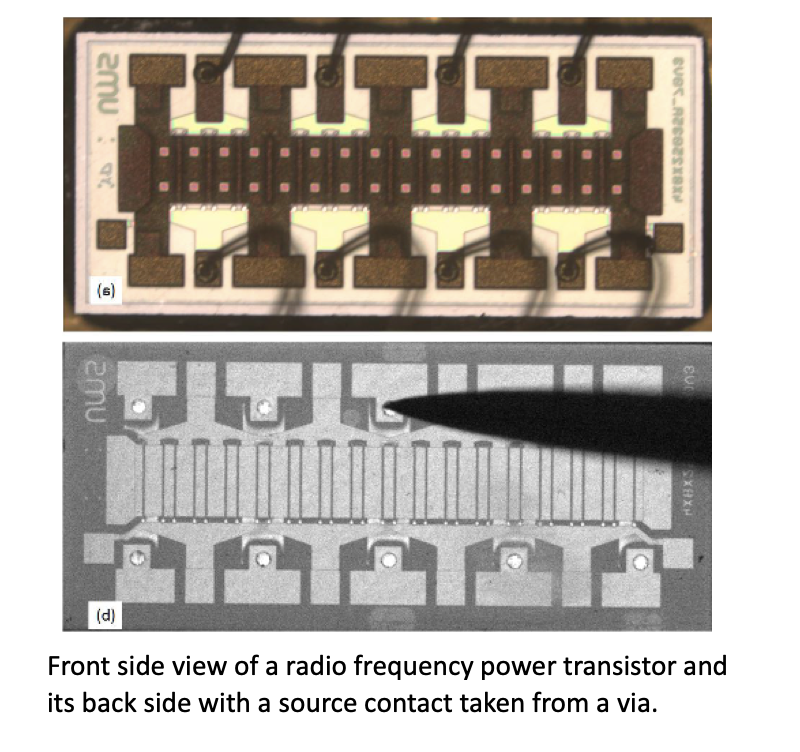
For several years, our work has followed a clear strategy focused on the study of the reliability and the physical analysis of the failures of power transistors of large gap technology. The applications concern both cutting components for DC-DC power conversion and also new generation radio frequency power components for radar, 5G and IOT applications. Efforts are focused on several fronts: the development of dedicated aging benches, fine electrical characterization, sample preparation and microstructural characterization. This work is carried out through numerous collaborations with industrial partners and academic laboratories.
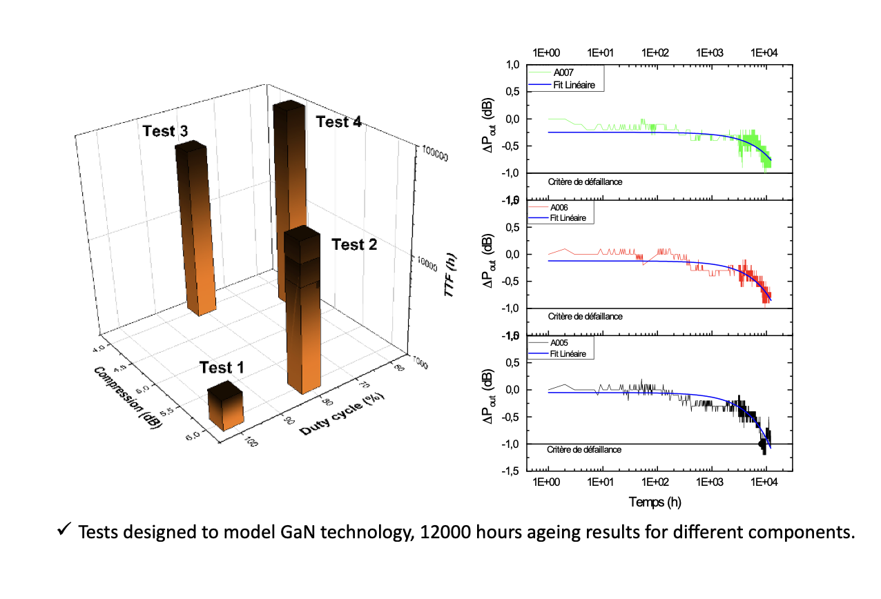
The fine electrical characterizations obtained during the aging steps performed on our measurement benches provide experimental data to establish aging models for GaN technology in particular. The objective is to better understand the failure mechanisms and the origin of the degradation of the transistors performances.
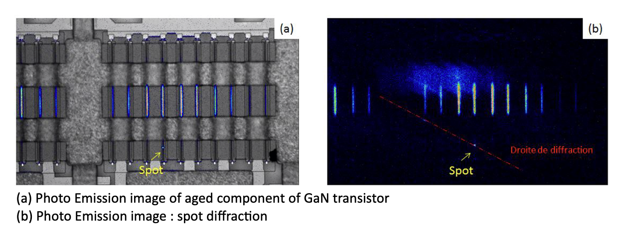
These electrical measurements are completed by steps of localization of the defects either by photon emission microscopy or by in-situ measurements on a portion of the transistor (finger or cell) in an instrumented FIB. In addition, EBIC (electron-beam induced-current) makes it possible to link the electrical performance of components to their structure at the atomic scale. Thanks to these measurement techniques, it is possible to locate the origin of traps. Our objective is to identify these electrical signatures by adapting our nanoscale trap measurement techniques and to find the correlation with atomic scale analyses (TEM and Atom Probe), the ultimate goal being to highlight the impurities at the supposed origin of the traps.


